PGD is a parameterized library for parallel graphlet decomposition (also known as motif counting) with many flexible interchangeable components (e.g., ordering strategies, representation, approximate/exact variants, etc.).
It is fast, parallel, parameterized, modular, and easy-to-extend library for efficient graphlet counting.
Highlight your project folder in the Project Manager window. Click > Annotate .
Place the components on the schematic grid. for alignment. orcad 16.6 tutorial
Right-click your schematic design cache or group-select components on your canvas. Select . Locate the PCB Footprint column. Highlight your project folder in the Project Manager window
Click > Cross Section to define your layer stackup (e.g., 2-layer or 4-layer board). for alignment
| Error Message | Likely Cause | Solution | | ------------------------------ | --------------------------------------------- | --------------------------------------------------------- | | "Netlist failed – missing pin" | Schematic symbol pin doesn't match footprint | Verify pin numbering in Part Editor. | | "Footprint not found" | PCB Footprint property misspelled or not set | Add PCB Footprint property in Capture (e.g., DPAK ). | | "DRC: Line to shape spacing" | Dynamic shape clearance violation | Increase shape clearance via Setup > Constraints > Spacing | | "Database lock" | Crash left .db lock file | Delete .db files in the project folder. |
). You can search through default libraries or download pre-made components from to save time. : Connect pins using the Place > Wire tool (Shortcut: Annotation
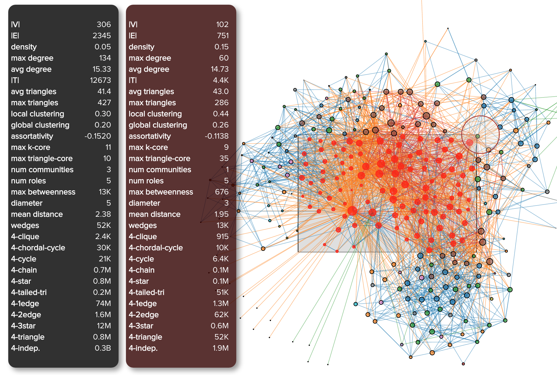
 Graphlet visualization from the diseasome network
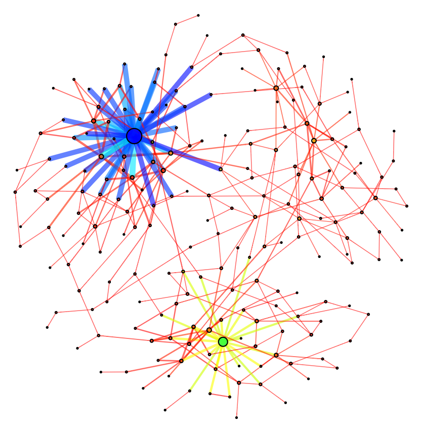
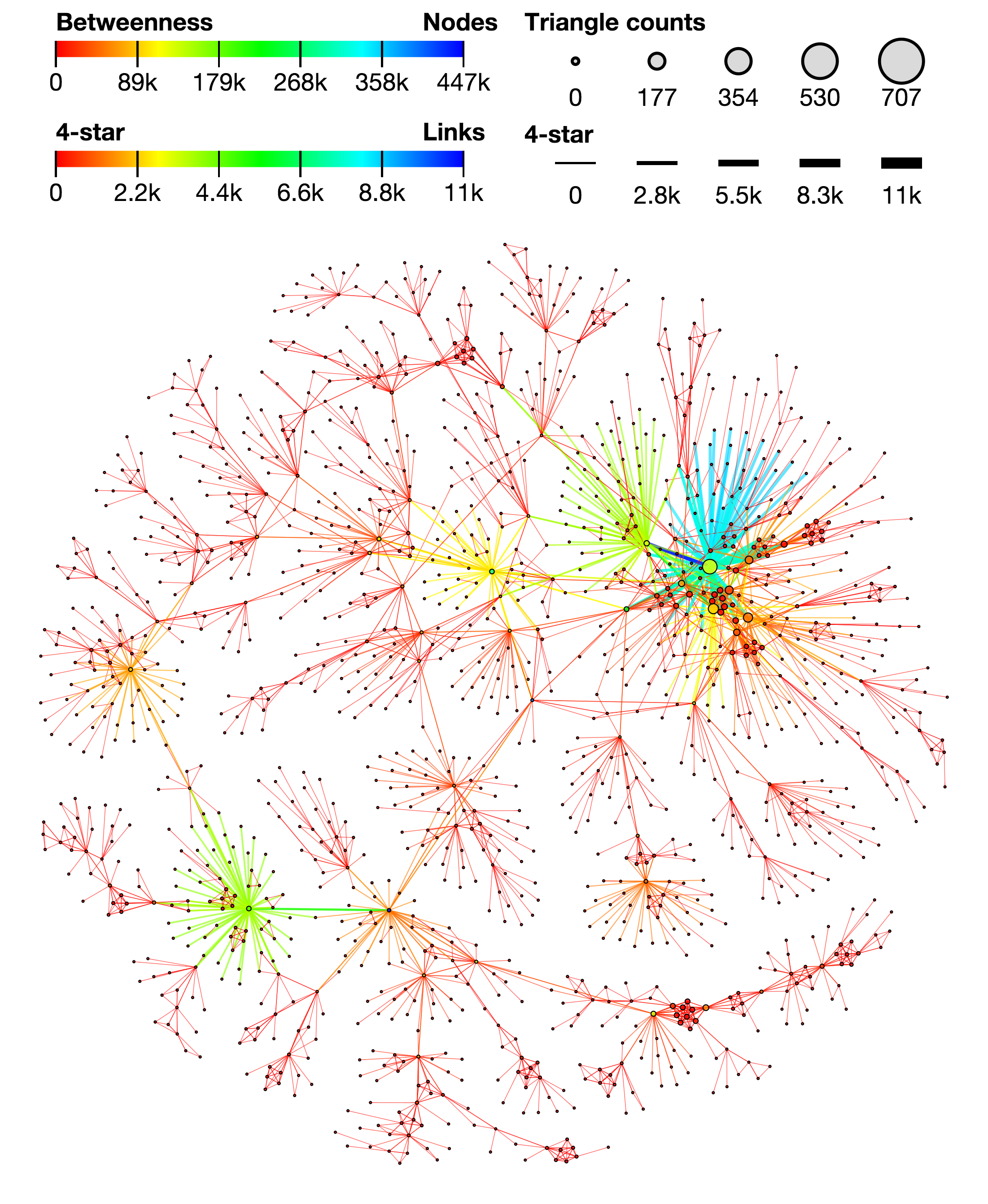
 Block Chung-Lu
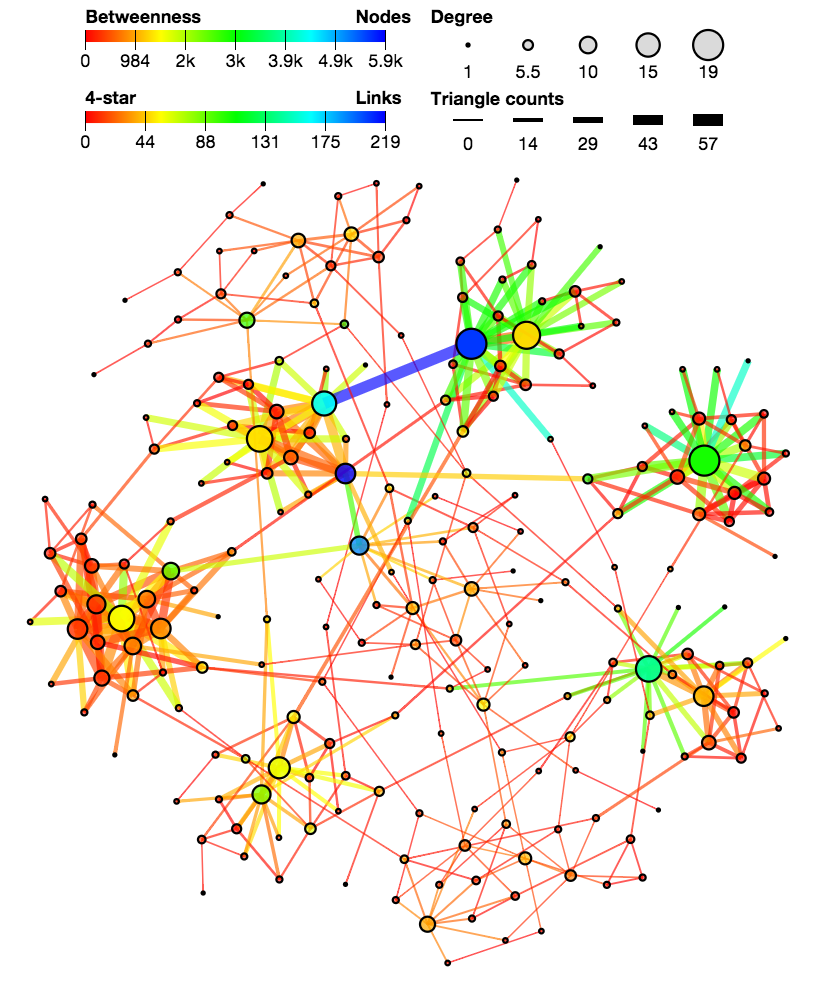
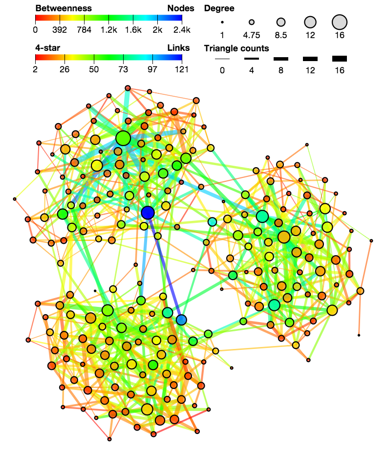 Block Erdos-Renyi
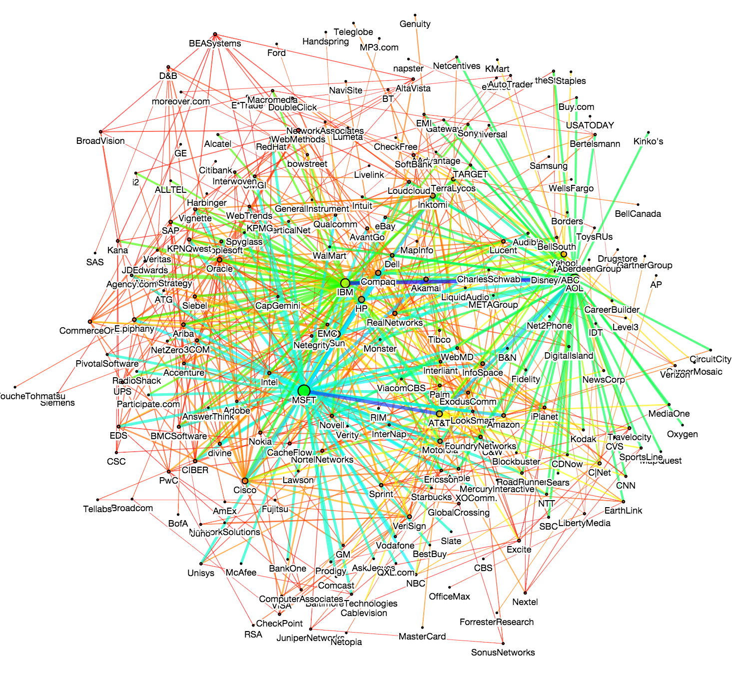
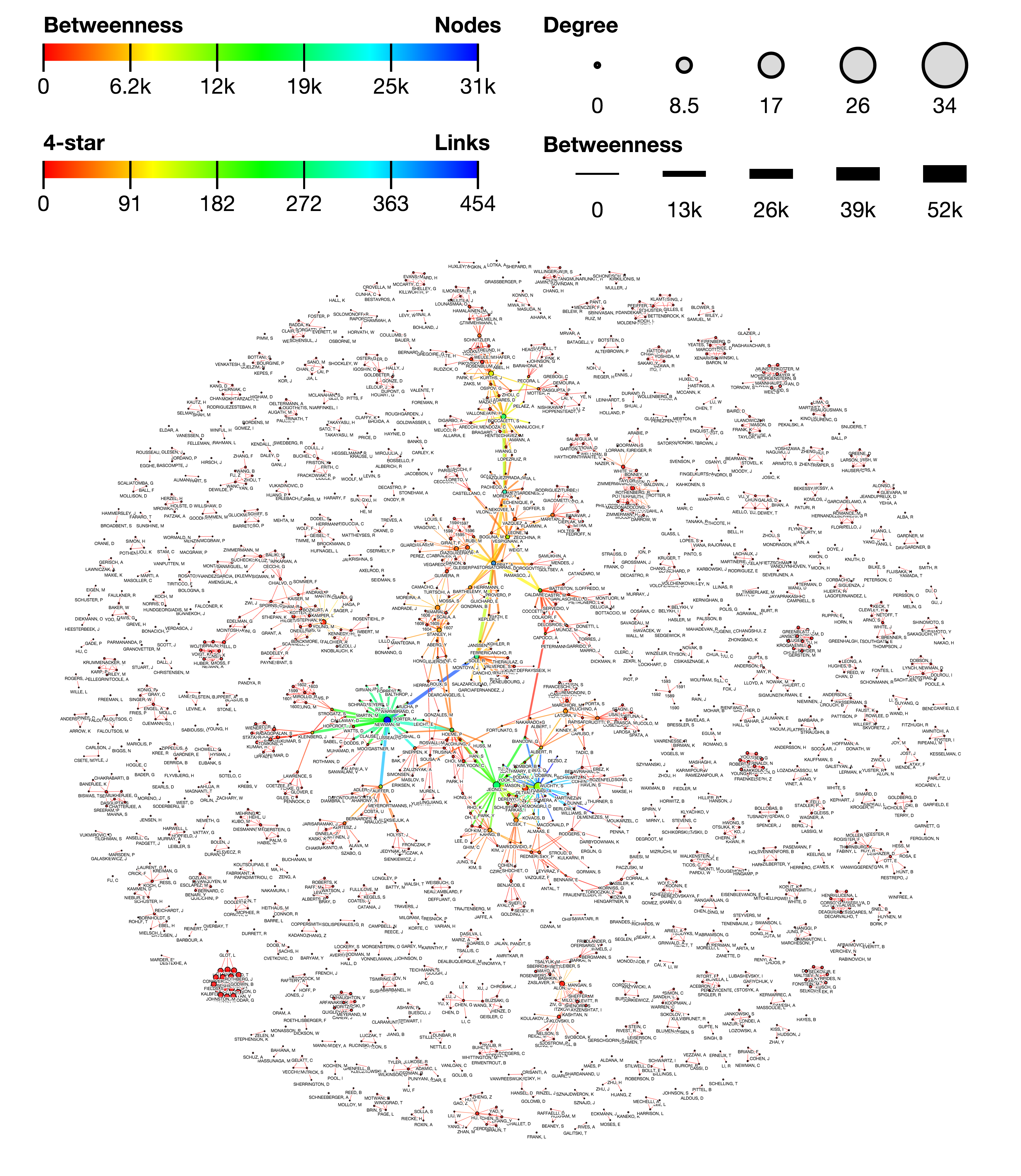 Spotting influential individuals in the collaboration graph from the network science community
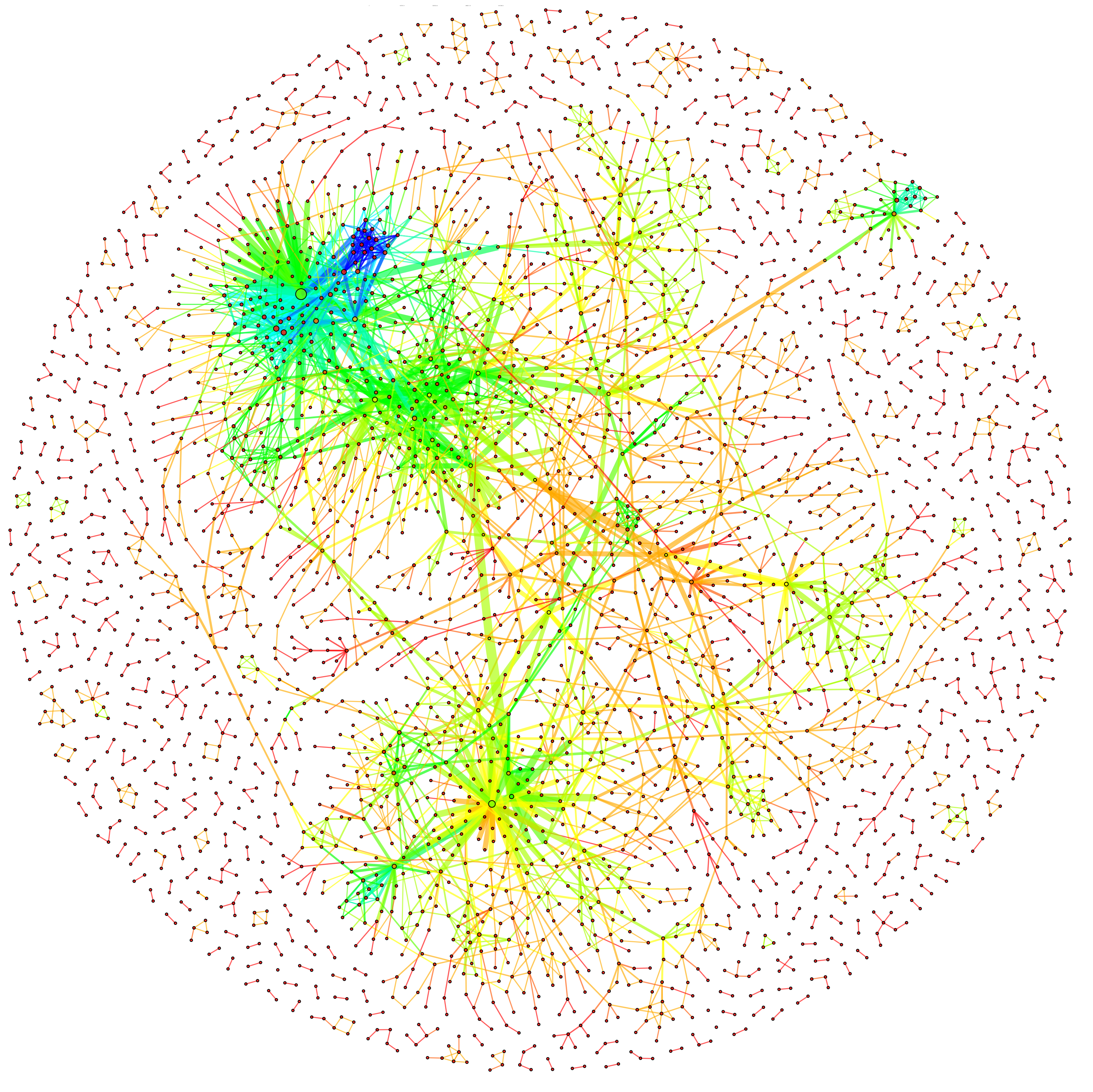
 High-performance library for large networks
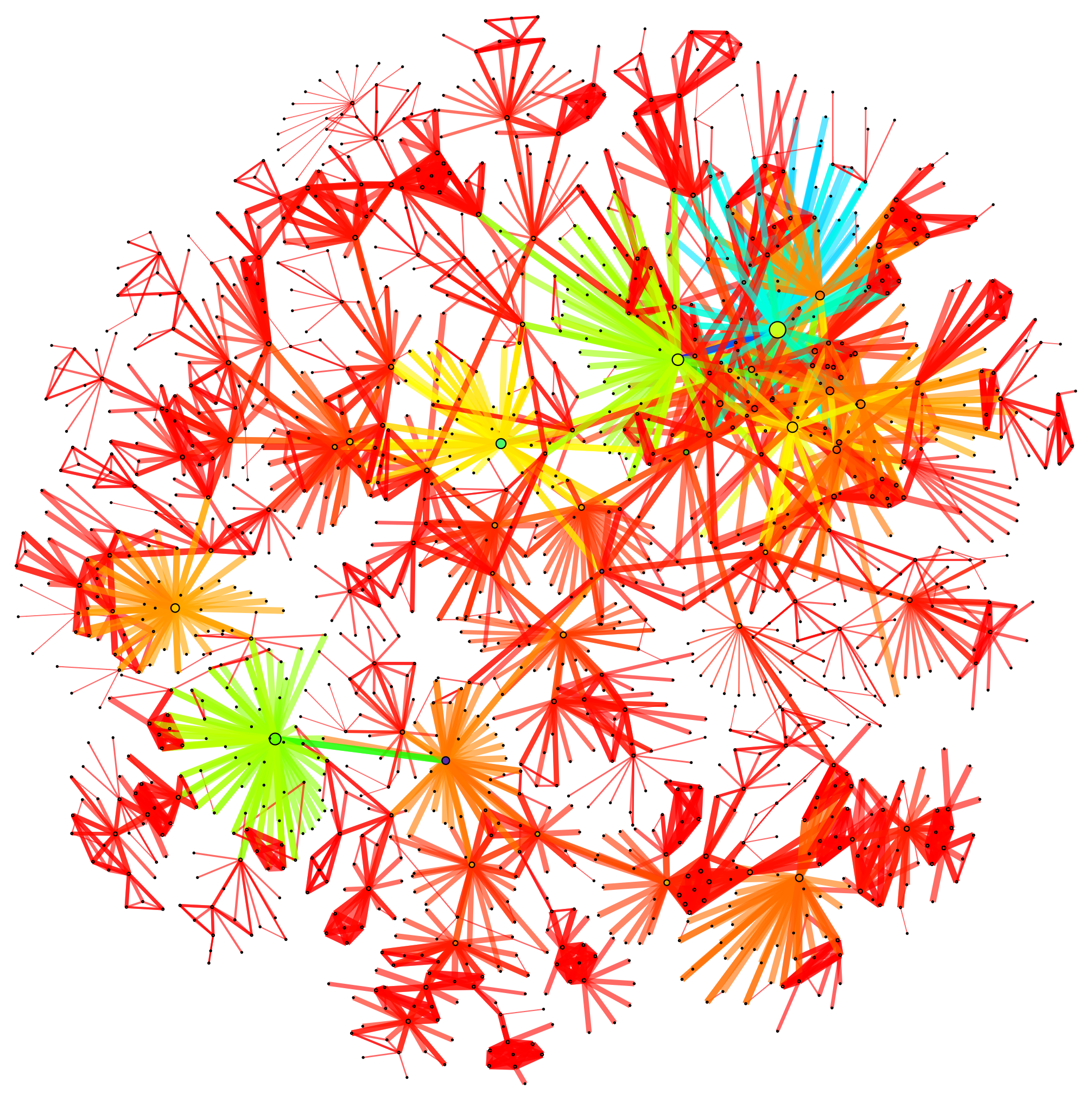
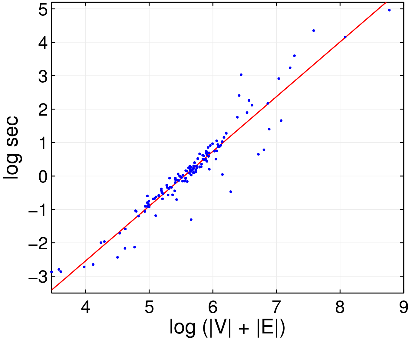
 Interactive graphlet decomposition